The image intensifiers are based in large part on the design for
commercial generation-II 25 mm devices. In order to increase the
photocathode lifetime a thin film of SiO2 is deposited over
the front face of the microchannel plate (MCP) assembly. This assembly
consists of two MCPs in the chevron configuration. The photocathode for
the visible cameras is trialkali type S20 and that for the Earth camera
is cesium iodide. The output electrons from the MCPs are
proximity-focused into a phosphor, JEDEC registration GH. The wavelength
for the phosphor spectral maximum is 525 nm. The decay times for the
phosphor emissions after shuttering the light source to the sensor are
 s and 1 s for decreases by
factors of 10-2 and 10-3, respectively. The image
intensifiers were manufactured by Science Applications International
Corporation at San Diego and the MCPs were supplied by Galileo
Electro-Optics Corporation. The overall amplification of the light input
is in the range of 105 and is determined by the potential
differences across the MCP assembly and between the MCP output face and
the phosphor. These bias voltages are controlled by ground command and
can be selected to values of 0 to 2500 V and 0 to 5700 V, respectively.
The gain of the image intensifier is sufficient to allow single-electron
events at the entrance aperture of the MCP to be recorded by the CCD. The
photocathodes can be back-biased in order to prevent current surges in
the MCPs due to an extremely bright light source or to eliminate the
effects of stray light from the science antennas that are mounted on the
spinning section of the spacecraft and hence periodically appear within
the fields-of-view of the cameras. This electronic shutter can be
activated by an alarm from the MCP current monitor and by spin phase
information from the spacecraft that is processed by the instrument
electronics.
s and 1 s for decreases by
factors of 10-2 and 10-3, respectively. The image
intensifiers were manufactured by Science Applications International
Corporation at San Diego and the MCPs were supplied by Galileo
Electro-Optics Corporation. The overall amplification of the light input
is in the range of 105 and is determined by the potential
differences across the MCP assembly and between the MCP output face and
the phosphor. These bias voltages are controlled by ground command and
can be selected to values of 0 to 2500 V and 0 to 5700 V, respectively.
The gain of the image intensifier is sufficient to allow single-electron
events at the entrance aperture of the MCP to be recorded by the CCD. The
photocathodes can be back-biased in order to prevent current surges in
the MCPs due to an extremely bright light source or to eliminate the
effects of stray light from the science antennas that are mounted on the
spinning section of the spacecraft and hence periodically appear within
the fields-of-view of the cameras. This electronic shutter can be
activated by an alarm from the MCP current monitor and by spin phase
information from the spacecraft that is processed by the instrument
electronics.
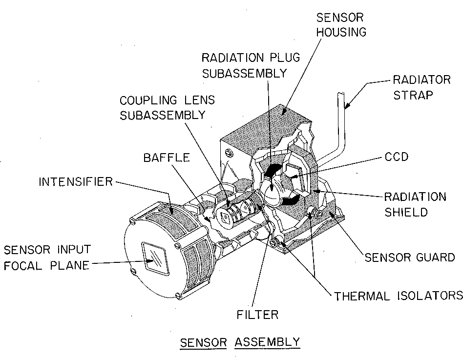
The image on the phosphor at the exit face of the intensifier is transferred to the CCD by a coupling lens assembly. A series of baffles prevents significant stray light scattering from the phosphor into the CCD (see Figure 7). For the sensor assemblies of the medium-resolution camera and Earth camera a folding mirror immediately follows the image intensifier in order to rotate the optical path by 90° for mechanical accommodation. A wideband transmission filter is mounted on the back of the coupling lens subassembly in order to limit chromatic aberration to acceptable values. The center of the filter passband and the passband width at half-maximum transmissions are 530 ± 25 nm. The coupling lenses are followed by a radiation plug subassembly, a 2 cm thick meniscus lens that can be mechanically translated along the chief ray for image focusing at the CCD.
The CCD is a Photometrics model PM516A which is manufactured by the
Loral-Fairchild Imaging Sensors Group. This device has a pixel size of
 m
m  m with a
  m
channel stop. The array size is 512 × 512 pixels. The baseline
operating mode sums a block of 2 × 2 pixels to yield one pixel. The
design of the CCD electronic controller is centered upon a custom-made
type-8000 gate array fabricated by United Technologies Microelectronics
Center.
m
channel stop. The array size is 512 × 512 pixels. The baseline
operating mode sums a block of 2 × 2 pixels to yield one pixel. The
design of the CCD electronic controller is centered upon a custom-made
type-8000 gate array fabricated by United Technologies Microelectronics
Center.
An important concern for the CCD is radiation degradation due to the fluxes of high-energy, penetrating protons in the inner radiation zone. Consequently, the sensor assembly was designed with a tantulum radiation shield that surrounds the entire solid angle around the CCD with the exception of the optical path. Along the optical path the radiation plug provides an equivalent minimum shielding of 5 gm/cm2, sufficient to stop protons with E 60 MeV. Calculations by Dyson [1991] as based upon the method of Janesick et al. [1991] indicate that the worstcase charge transfer efficiency (CTE) for a single pixel of the CCD is 0.99991 for the 300 kRad total radiation dose during a nominal three-year mission. The CTE is the measure of the performance in transferring charge from one pixel to the next pixel in the process of shifting the pixel charge packet out for A/D conversion. Thus for the pixel in row 512 and column 512, (0.99991)1024 = 0.91 of the charge that had accumulated in this pixel during image integration is received by the amplifier.
In order to further minimize the effects of radiation damage by energetic
ions the CCD is passively cooled to a temperature of about -90° C by
thermal coupling to a radiator through the radiator strap (see
Figure 7). The CCD is connected to
electronics and thermally isolated as much as feasible with the use of
thirteen 76  m diameter
constantan wires. At this low temperature the time constant for electron
captivation in the radiation-induced traps increases to times exceeding
that for image readout. That is, the electron remains in the trap and is
not picked up in the signal charge packet.
m diameter
constantan wires. At this low temperature the time constant for electron
captivation in the radiation-induced traps increases to times exceeding
that for image readout. That is, the electron remains in the trap and is
not picked up in the signal charge packet.